

This page includes selected results from our research. You can navigate between different subjects listed below. For a complete list of publications go to the publications page.
Band Alignment of Two-dimensional Semiconductors

We present a comprehensive study of the band alignments of two-dimensional (2D) semiconducting materials and highlight the possibilities of forming momentum-matched type I, II, and III heterostructures, an enticing possibility being atomic heterostructures where the constituent monolayers have band edges at the zone center, i.e., Γ valley. Our study, which includes the group IV and III-V compound monolayer materials, group V elemental monolayer materials, transition-metal dichalcogenides, and transition-metal trichalcogenides, reveals that almost half of these materials have conduction and/or valence band edges residing at the zone center. Using first-principles density functional calculations, we present the type of the heterostructure for 903 different possible combinations of these 2D materials which establishes a periodic table of heterostructures.
Wavefunction Engineering of van der Waals Heterostructures
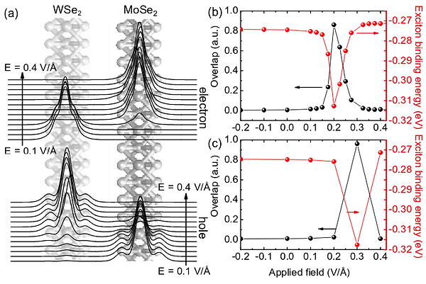
We investigate excitons in stacked transition metal dichalcogenide (TMDC) layers under perpendicularly applied electric field, herein MoSe2/WSe2 van der Waals heterostructures. Band structures are obtained with density functional theory calculations, along with the electron and hole wave functions in conduction and valence bands, respectively. Although the type-II nature of the heterostructure leads to fully charge separated inter-layer excitons, charge carriers distribution among the layers is shown to be easily tunable by external field. Our results show that moderate values of electric field produce more evenly distributed wave functions along the heterostructure, thus enhancing both the inter-layer exciton binding energy and, most notably, its oscillator strength.
Dielectric Nanocapacitor Model
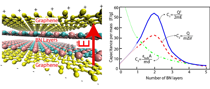
We investigate a nanoscale dielectric capacitor model consisting of two-dimensional, hexagonal h-BN layers placed between two commensurate and metallic graphene layers using self-consistent field density functional theory. The separation of equal amounts of electric charge of different sign in different graphene layers is achieved by applying an electric field perpendicular to the layers. The stored charge, energy, and the electric potential difference generated between the metallic layers are calculated from the first principles for the relaxed structures. Predicted high-capacitance values exhibit the characteristics of supercapacitors. The capacitive behavior of the present nanoscale model is compared with that of the classical Helmholtz model, which reveals crucial quantum size effects at small separations, which in turn recede as the separation between metallic planes increases.
Planar nanocapacitor
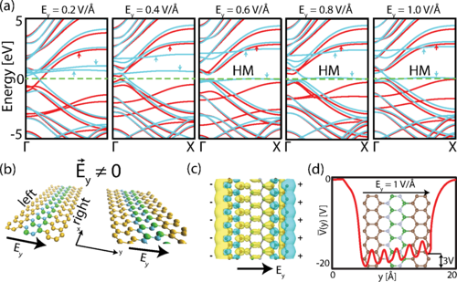
We propose a model for planar nanoscale dielectric capacitors consisting of a single layer, insulating hexagonal boron nitride (BN) stripe placed between two metallic graphene stripes, all forming commensurately a single atomic plane. First-principles density functional calculations on these nanoscale capacitors for different levels of charging and different widths of graphene-BN stripes mark high gravimetric capacitance values, which are comparable to those of supercapacitors made from other carbon-based materials. Present nanocapacitor models allow the fabrication of series, parallel, and mixed combinations which offer potential applications in two-dimensional flexible nanoelectronics, energy storage, and heat-pressure sensing systems.